
Make Noise front panels are easily recognizable by the wonderful indicator lights that seem to be integrated into the front panels themselves. I’ve been wanting to experiment with this technique for some time now. And so a while ago I designed a concept for illuminated blind plates. The prototypes arrived recently and I’ve been showing them off on different social media. Some people on Reddit were interested in learning more about them and so I decided to put up a little tutorial. I will be covering two main topics. First I will explain what the general working principle behind this kind of indicator light is. Secondly I’ll shine some light (pun intended) on how I design my graphics and how I get them printed on the front panels.

The magic explained
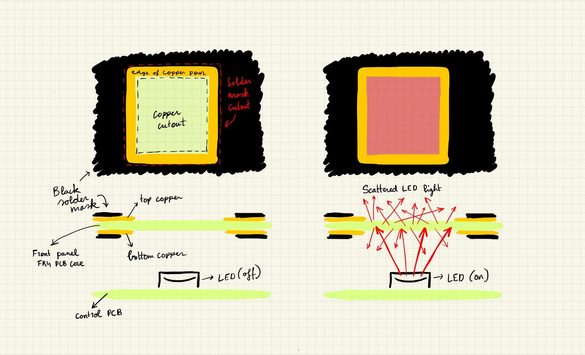
So, how do these “Make Noise” style indicator lights work? It’s actually not rocket science. These types of front panels are actually standard PCB’s with a matte-black solder mask. The reason for this is that the most commonly used substrate/core material for PCB’s, FR4, has optical properties much akin to that of frosted glass (albeit with a slight green tinge). So, when you put a light source behind it, the light is diffused. This is exactly what Make Noise does to implement their famous indicator lights. The stack-up will look like this:
- A front panel made out of PCB material
- Usually, the PCB will have copper fills on the top and bottom layers
- There’s a copper cutout (on all layers of the PCB), creating a window to let through light
- Slightly larger, there’s a solder mask cut out, exposing the copper to be viewed. This creates a nice metallic frame for the indicator light.
- By selecting an Electroless Nickel Immersion Gold (ENIG) plating as a finishing option, the exposed copper of the PCB will get a nice golden look.
- On the control PCB, placed under the front panel there will be an LED whose placement is aligned with the “window” in the front panel.
The optics behind it in a nutshell
The light emitted by the LED is scattered by the FR4 material. The reason for this is, in a nutshell, that the inhomogeneities in the FR4 substrate are significantly larger than the wavelengths of the emitted light. Meanwhile, the FR4 does not completely absorb the LEDs light, letting a good portion of the intensity pass through (while being scattered). As a result, you will see the LEDs light being distributed quasi homogenously over the surface of the copper cutout, as opposed to a clear image of the LEDs bulb if the FR4 material wouldn’t be present in our line of view (Here I am that assuming the opening angle of the LED and the cutout’s surface are well matched of course).
The thickness of the PCB material will also have a role to play in this story. The total amount of light that reaches the other side of the PCB is proportional to 10^(-L) with L being the thickness of the PCB, as described by the Beer-Lambert law. Simply put, the thickness of the PCB has a very large impact on the amount of light that is transmitted. Luckily, a standard 1.6mm thickness seems to yield workable results. Should you find that a higher light transmission is desirable, reducing the thickness of the PCB to 1.2mm or even 1mm should yield a dramatic impact. Do note that the tradeoff will be a reduced stiffness of the front panel and reduced light diffusion.
Pushing the concept further
Let’s say that we place LEDs on the back of the front panel, which has a large copper cutout (so most of it acts as a frosted glass panel). Remember, this is something that’s perfectly feasible, as the front panel is a regular old PCB. When the front panel is mounted in a rack, it will thus illuminate a small closed-off volume. The light will start to mix and spread throughout the volume of the case because of all these diffuse reflections because the inside of the rack will act as a diffusely reflective surface. Of course for each reflection the intensity of the light will be partially absorbed. A dark surface will absorb more than a light surface. Even so, when making use of bright LEDs, there should be plenty of light left after a first diffuse reflection. The majority of this reflected light should end up back on the surface of the “frosted glass” front panel. For the outside viewer it should look like the panel is lit up from the inside. A high-performance version of this concept is used in integrating spheres, which are used to thoroughly homogenize light sources (often in a scientific context).

The LED circuitry
Below you’ll find the schematic that I ended up implementing. It has the following features:
- Six high brightness RGB LEDs (to be placed on the bottom of the PCB)
- The R, G and B LEDs have individual pinouts. This means I can drive each color separately
- I have three diodes in series between 12V and GND
- I have three diodes in series between GND and -12V
- This way I’m getting the most amount of light for the same current, while retaining some voltage headroom so I can use a standard resistor to set the diode current.
- Solder jumpers allow you to choose which colors are powered, so you can set the color of the light to the mood you’re looking for in your rack.
- There are two power headers, one for connecting to the rack’s power supply bus, the other for daisy-chaining that power to the next illuminated panel. This way you don’t eat up all the power connectors on your bus board.
- All components are specified as SMT as through-hole connections would mess-up the aesthetic of the panel.
Please note that this schematic was co-designed with the layout, going back and forth between the two. For example, I originally wanted to have regular jumpers instead of the solder jumpers because they are more practical. Unfortunately, these took up too much space and would’ve been visible through the FR4 material of the PCB.

Designing my graphics
Here’s a rundown of how I design all of my front panel art:
- I make my drawings on my iPad pro with an Apple pencil in an app called Goodnotes. This is actually not a graphical design app, but intended for taking notes. I use this app almost daily for work. I like how its simplicity inspires me to be creative. When I’m not free drawing, I will take an inspiring picture and trace it (that’s what I did for this blank panel).
- Next, I export this drawing to a PDF file and open it in Inkscape for post-processing. In Inkscape I define the size of the document to be equal to the size of the front panel, and I make the design fit to its destination format. In this case I’ve also applied some masking, mirroring and rotation to create an interesting psychedelic pattern.
- Now that I have a design with well-defined dimensions and ratio, I export it to png at 600 dpi, with the export area being set to the document outline.
- Finally, I will use KiCad’s bitmap to component converter to convert my graphics to a component footprint*. This footprint is then assigned to a dummy component in the schematic so that it will appear in the layout when you update your PCB.
(* the bitmap converter can only make footprints on the silkscreen and solder mask layers. If you need your graphics to be on the copper layer, open up the footprint file with a text editor and replace “F.Silk” or “F.Mask” with “F.Cu”)
In the slideshow below you’ll find illustrations of each step in my process.

The original silly picture of me with two jeweler’s magnifiers over my eyes. 
A traced doodle of the original picture. I did this for fun one night, not really sure what I was going to use it for. 
A first set of drafts, not really sure yet what route I’d be going down. 
Second and final set of concepts. A friend suggested that I introduce symmetry, and that was an excellent suggestion. This lead me to the final design. 
The final design! :) 
Use KiCad’s bitmap to component converter to create a footprint 
Add the footprint containing your graphics to a component in your schematic. When you update your PCB this will make your graphics appear in the layout.
Making the graphics work in KiCad
Ok, so now I have these nice graphics in my layout, what to do next? Here’s a list of all steps taken:
- Define the outer dimensions of the blank panel on the Edge Cut layer.
- Place the mounting slots according to Doepfer’s construction details.
- Position the graphics on the top copper and top solder mask layers to make sure that my graphics are visible through the solder mask as copper features
- Place a copper cutout (both for the top and bottom layers in the central region of my graphics, allowing light to pass through in this region.
- Place copper fills along the edges of the panel, both on the top and bottom layers (the non-transparent regions).
- Layout the LED circuitry in the non-transparent regions.
- Export to Gerber files and order prototypes.
In the slideshow below you can have a look at the layout of my copper and solder mask layers.

Top copper. Contains my graphics, a copper cutout in the center and copper fills all around that. 
Bottom copper, containing the LED circuitry. In the center there’s a copper cutout. The tracks that connect the left and right hand sides of the LED circuitry are aligned with the features of the graphics on top, making them virtually invisible to the observer. 
Top solder mask cutout. This contents is the union of the graphics on the top copper and the copper cutout. 
Bottom solder mask cutout
Adding high-quality graphics in other CAD software
If you’re not using KiCad, another great way of adding high-quality graphics to a PCB layout is through creating a custom font. When working in Altium Designer, this is my go-to technique, but you can do it in any CAD software that supports using TrueType fonts. Have a look at this great tutorial that explains this technique.
Pics, cause it happened!
When I hold the prototypes in front of different light sources, I observe promising results w.r.t transmissive and diffusive properties. Below are some pictures for you to enjoy :).

Holding up the prototype to a sunny sky. 
Close up detail of the copper graphics. 
Close up of the LED circuitry. You can see that it’s all located on the non-transparent regions. 
Holding the prototype in front of the LEDs of my Turing Machine module. The blue light is coming from my MDLRcase’s power supply. 
Putting the prototypes closely over a light source (my Roger Linnstrument in this case) proves that some distance is desirable to achieve sufficient diffusion/homogenization.
Conclusion
For now, I’m very happy with the quality of my prototypes. Of course, the next step is to order the components for the LED circuit and to eat my own damn pudding (because that’s where the proof lies after all). I’ll post a follow-up when I do.
I really hope you enjoyed my tutorial so far. Please know that it’ll make my day if you leave a comment below!
Stay safe and stay healthy!
Update
Find some pictures of the results in the articles below :)
